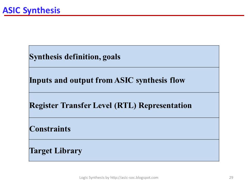
Design Objects


1.    Design Objects

Design objects which are regularly used w.r.to design are design is explained below.

Wire load models for synthesis


9.1. Wire load models for synthesis

Wire load modeling allows us to estimate the effect of wire length and fanout on the resistance, capacitance, and area of nets. Synthesizer uses these physical values to calculate wire delays and circuit speeds. Semiconductor vendors develop wire load models, based on statistical information specific to the vendors’ process. The models include coefficients for area, capacitance, and resistance per unit length, and a fanout-to-length table for estimating net lengths (the number of fanouts determines a nominal length).

Wire load models


1.    Wire load models

Extraction data from already routed designs are used to build a lookup table known as the wire load model (WLM). WLM is based on the statistical estimates of R and C based on “Net Fan-out”.

Operating Condition: Operating Temperature Variation

8.3. Operating Temperature Variation

Temperature variation is unavoidable in the everyday operation of a design. Effects on performance caused by temperature fluctuations are most often handled as linear scaling effects, but some submicron silicon processes require nonlinear calculations.

Operating Condition: Supply Voltage Variation

8.2. Supply Voltage Variation

The design’s supply voltage can vary from the established ideal value during day-to-day operation. Often a complex calculation (using a shift in threshold voltages) is employed, but a simple linear scaling factor is also used for logic-level performance calculations.

Operating Condition: Process Variation

8.1. Process Variation

This variation accounts for deviations in the semiconductor fabrication process. Usually process variation is treated as a percentage variation in the performance calculation. Variations in the process parameters can be impurity concentration densities, oxide thicknesses and diffusion depths. These are caused bye non uniform conditions during depositions and/or during diffusions of the impurities. This introduces variations in the sheet resistance and transistor parameters such as threshold voltage. Variations are in the dimensions of the devices, mainly resulting from the limited resolution of the photolithographic process. This causes (W/L) variations in MOS transistors.

Operating conditions


1.     Operating conditions

Sources of variation in performance of a chip are due to:

Ø  Process variation (P)

Ø  Supply voltage (V)

Ø  Operating Temperature (T)

.lib: Cell description


7.2.4. Cell description


A cell description in the logic library contains variety of attributes describibing the function, timing, power and any other related information of the cell.

.lib: Wire Load Models


7.2.3.3. Wire Load Models

Wire load models contain informations that synthnesis tool utilizes to estimate interconnect wiring delays during logic synthesis phase of the design. Logic library includes several models approarpriate to different sizes of the design.

.lib: Operating Conditions:


7.2.3.2. Operating Conditions:

This section models the environmental variations of IC. These are known as Process, Voltage, and temperature variations. In short it is called PVT.


A set of values of PVT is known as operating condition. A logic library is characterised for one set of operating condition. Generally there are different libraries specific to different operating condition. There are three operating conditions very commonly used in ASIC synthesis and implementation. Based on the affect on cell delay due to the variation in PVT these classifications are made.

They are:

Ø  worst (also called ‘max’ or ‘slow’)à library in which cells are characterised for maximum delay

Ø  best(also called ‘min’ or ‘fast’)àlibrary in which cells are characterised for minimum delay

Ø  nominal(also called ‘typical’ or ‘normal’)àlibrary in which cells are characterised for typical delay

Eg.:

  /* Operation Conditions */

  nom_process                     : 1.00;

  nom_temperature                 : 125.00;

  nom_voltage                     : 0.95;


  voltage_map (VDD,0.95);

  voltage_map (VSS,0.00);


  define(process_corner, operating_conditions, string);

  operating_conditions (slow) {

    process_corner : "SlowSlow";

    process       : 1.00;

    voltage       : 0.95;

    temperature   : 125.00;

    tree_type     : balanced_tree;

  }
  default_operating_conditions : slow;

.lib: Environment Description


7.2.3. Environment Description

7.2.3.1. Scaling Factors:
The scaling factors (also called as K-factors) are multipliers that provide flexibility for derating the delay values based on PVT.  If PVT changes by a particular value then how to calculate parameter like cell delay or net delay? using these K-factors that can be accomplished.

.lib: Library level attributes


7.2.2. .lib: Library level attributes

Library level attributes section explains technolgy type, date, revision. It also gives units of volt, amps, time, capacitance etc which are used in the library.
 

Eg.:

  /* General Attributes */

  technology                        (cmos);

  delay_model                     : table_lookup;

  in_place_swap_mode              : match_footprint;

  library_features                  (report_delay_calculation,report_power_calculation);


  /* Units Attributes */

  time_unit                       : "1ns";

  leakage_power_unit              : "1nW";

  voltage_unit                    : "1V";

  current_unit                    : "1mA";

  pulling_resistance_unit         : "1kohm";

  capacitive_load_unit              (1,ff);

Logic Library


7.1 Logic Library

Logic synthesis relevant information are contained in logic libraries. Logic libraries does not contain any physical information of the logic gates. Logic library is a text file. Initially its development were done by a company called “liberty” which was later got acquired by EDA company Synopsys. Hence usual extension of logic libray is .lib and is known as liberty format logic library. This is now universally accepted and used by all fabrication houses and EDA companies.
 
Logic library has timing, area and power information pertaining to all logic gates. These characteristics include information such as cell names, pin names, delay arcs, and pin loading.
 
The technology library also defines the conditions such as the maximum transition time for nets, maximum capacitance and maximim fanout loading. These conditions are called design rule constraints.
 
In addition to cell information and design rule constraints, specify the operating conditions and wire load models specific to that technology are specified in technology library.
 
Net delay models in logic libraries are calculated from different models known as:
Ø  Nonlinear delay models (NLDMs)
Ø  Composite Current Source (CCS) models
 
7.2 Basics of Logic Library (.lib)
The contents of logic library can be broadly classified as below:
Ø  Library group
Ø  Library level attributes
Ø  Environment Description
Ø  Cell description
 
7.2.1. Library group
This gives part specifies general information such as library name regarding library.

The Need for Speed: Understanding Design Factors that Make Multi-core Parallel Simulations Efficient


by Shobana Sudhakar & Rohit Jain, Mentor Graphics
Running a parallel simulation may be as easy as flipping on a switch with the progressive and maturing solutions available today, but do people really take full advantage of the technology? It is true that in some scenarios the overhead of communication and synchronization needed for parallel simulation can negate any substantial performance gains. However, there are scenarios where deploying the parallel simulation technology can provide tremendous benefit. A long running simulation that exercises large blocks of a design concurrently and independently is one good example.
Designers need to be aware of the factors that can inhibit the advantages of parallel simulations, even in these best case scenarios; the main factor being inflexibility due to the way designs are modeled today. This article focuses on these factors and is an effort to educate on best design principles and practices to maximize the advantage of simulation with parallel computing. The discussion also extends to the three main fundamental features of parallel simulations, viz., load balancing, concurrency and communication. Designers need to understand how their designs run in simulation with these factors to ensure they get the maximum out of parallel simulations....
Read complete article from Mentor Graphics:  The Need for Speed: Understanding Design Factors that Make Multi-core Parallel Simulations Efficient

Monitors, Monitors Everywhere – Who Is Monitoring the Monitors?


by Rich Edelman and Raghu Ardeishar, Mentor Graphics
The reader of this article should be interested in predicting or monitoring the behavior of his hardware. This article will review phase-level monitoring, transaction-level monitoring, general monitoring, in-order and out-of-order transactionlevel monitors, A protocol specific AXI monitor written at the transaction-level of abstraction will be demonstrated. Under certain AXI usages, problems arise. For example partially written data may be read by an overlapping READ. This kind of behavior cannot be modeled by the "complete transaction" kind of monitor; it must be modeled by a phase-level monitor. All of these monitoring and scoreboard discussions can be widely applied to many protocols and many monitoring situations.
The task of a monitor is to monitor activity on a set of DUT pins. This could be as simple as looking at READ/WRITE pins or as complex as a complete protocol bus, such as AXI or PCIe. In a very simple case a monitor can be looking at a set of pins and generating an event every time there is a change in signal values. The event can trigger a scoreboard or coverage collector. This monitor is typically very slow and not very useful as it generates a lot of irrelevant data.....
Read complete article from Mentor Graphics:  Monitors, Monitors Everywhere – Who Is Monitoring the Monitors?

Flexible UVM Components: Configuring Bus Functional Models

by Gunther Clasen, Ensilica

Modern object-oriented testbenches using SystemVerilog and OVM/UVM have been using SystemVerilog interface constructs in the testbench and virtual interfaces in the class based verification structure to connect the two worlds of static modules and dynamic classes. This has certain limitations, like the use of parameterized interfaces, which are overcome by using Bus Functional Models. BFMs are now increasingly adopted in UVM testbenches, but this causes other problems, particularly for complex BFMs: They cannot be configured from the test environment, thus significantly reducing code reuse.
This article shows a way to write BFMs in such a way that they can be configured like any other UVM component using uvm_config_db. This allows a uniform configuration approach and eases reuse. All code examples use UVM, but work equally with the set_config_*() functions in OVM......
Read complete article from Mentor G raphics: Flexible UVM Components: Configuring Bus Functional Models

NoC Generic Scoreboard VIP

by François Cerisier and Mathieu Maisonneuve, Test and Verification Solutions

The increase of SoC complexity with more cores, IPs and other subsystems has led SoC architects to demand more from the main interconnect or network-on-chip (NoC), which is thus becoming a key component of the system. Power management, multiple clocks, protocol conversions, security management, virtual address space, cache coherency are among the features that must be managed by main interconnect and that demand proper verification.
In addition, IP reuse and NoC generation solutions have enabled the conception of new SoC architectures within months or even weeks. Simple point-to-point scoreboard methodology is taught in most good verification methodology books and tutorials. However, building a generic verification solution for an SoC interconnect that can quickly adapt to any bus protocols and SoC architectures, and can deal with SoC advanced features, requires much more than dealing with point-to point transaction matching.....
Read complete article from Mentor graphics:  NoC Generic Scoreboard VIP

Making it Easy to Deploy the UVM


by Gaurav Jalan, SmartPlay Technologies, and Pradeep Salla, Mentor Graphics
Until recently, the semiconductor industry religiously followed Moore's Law by doubling the number of transistors on a given die approximately every two years. This predictable growth allowed ecosystem partners to plan and deal with rising demands on tools, flows and methodologies. Then came the mobile revolution, which opened up new markets and further shifted the industry's focus to consumers. The diversified nature of this market posed many, often conflicting development challenges: How to speed time to market while building products rich in functionality? How to boost performance while keeping both power consumption and cost at modest levels? Wading through these questions contributed to a multifold increase in verification complexity....
Read complete article from Mentor Graphics:  QVM: Enabling Organized, Predictable, and Faster Verification Closure

Making it Easy to Deploy the UVM

by Dr. Christoph Sühnel, frobas GmbH

The Universal Verification Methodology (UVM) is becoming the dominant approach for the verification of large digital designs. However, new users often express concern about the effort required to generate a complete and useful UVM testbench. But the practical experience collected in numerous OVM and UVM projects during the last few years shows a different view. The UVM is a very suitable methodology for any kind of design and implementation, i.e. ASIC and FPGA due to the availability of the UVM library and the well-defined testbench structure. This allows the automation of essential steps in employing the UVM.
This article describes an UVM approach reducing testbench implementation effort, guaranteeing an early success and streamlining the processing of the test results. Depending on the number of functional interfaces and the design complexity up to 6 weeks of implementation effort or even more can be saved. A runnable UVM testbench will be handed over to the verification team at the very beginning of the project. The verification engineers have to implement only the corresponding drivers, monitors and functional coverage models. Later on the scoreboards needed have to be architected and implemented.....
Read complete article from Mentor Graphics:  Making it Easy to Deploy the UVM

Confidence in the Face of the Unknown: X-state Verification


by Kaowen Liu, MediaTek Inc., and Roger Sabbagh, Mentor Graphics
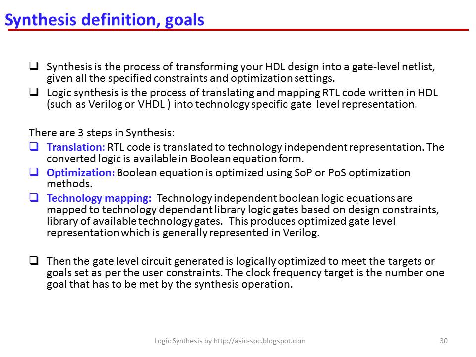
Unknown signal values in simulation are represented as X-state logic levels, while the same X-states are interpreted as don't care values by synthesis. This can result in the hazardous situation where silicon behaves differently than what was observed in simulation. Although the general awareness of X-state issues among designers is good, gotchas remain a risk that traditional verification flows are not well equipped to guard against. The unknown simulation semantics of X has two oft discussed pitfalls: X-pessimism and X-optimism.
X-optimism is most worrisome as it can mask true design behavior by blocking the propagation of X-states and instead propagating a deterministic value through the design in simulation, when in reality various possible values will be seen in the hardware. If the unexplored values cause the design to malfunction, then X-optimism has masked a design bug that will only be discovered in silicon.......
Read complete article from Mentor Graphics:  Confidence in the Face of the Unknown: X-state Verification

Verifying High Speed Peripheral IPs


by Sreekanth Ravindran and Chakravarthi M.G., Mobiveil
High speed serial interconnect bus fabric is the SoC backbone, managing dataflow and keeping up with the dynamic bandwidth requirements of high speed applications. Verification of high speed interconnect IPs presents critical challenges not only in terms of complying with standards, but also in ensuring that the design is robust and flexible enough to handle and manage a large amount of time-critical data transfers. Acquiring such expertise requires years of verification experience. In this article, Silicon IP and platform enabled solution provider Mobiveil shares its story of verifying high speed bus protocol standards like PCI Express and Serial RapidIO, including what considerations are required when verifying high speed designs. In addition, Mobiveil highlights the benefits of using the Mentor Graphics Questa Verification Platform, including Questa Advanced Simulator, Questa CoverCheck, and Questa Clock-Domain Crossing (CDC) Verification, which together facilitates smart functional verification, debug and reporting of the high speed designs....
Read complete article from Mentor graphics: Verifying High Speed Peripheral IPs

Non-invasive Software Verification using Vista Virtual Platforms


by Alex Rozenman, Vladimir Pilko, and Nilay Mitash, Mentor Graphics
With the SoCs now supporting Multi-Core processors, complex ASICs and combinations that include systems on a board, SoC implementations now become an ever growing challenge for software development. Software development has to be supported not only by the inclusion of an RTOS, but, many SoC providers now have to leverage upon the Bare-Metal concept to achieve the necessary demands of today's SoCs. However, there still exists a huge chasm in the software development arena that addresses both the need to be able to verify not only the sw/hw interactions, but, also the software itself in a hardware context. This has become almost a necessity in today's "security" based systems marketplace....
Read complete article from Mentor Graphics:  Non-invasive Software Verification using Vista Virtual Platforms

Power Up Hardware/Software Verification Productivity


by Matthew Ballance, Mentor Graphics
Today's complex designs increasingly include at least one, and often more, embedded processors. Given software's increasing role in the overall design functionality, it has become increasingly important to leverage the embedded processors in verifying hardware/software interactions during system-level verification. Comprehensively verifying low-level hardware/software interactions early in the verification process helps to uncover bugs that otherwise would be uncovered during operating system or application bring-up – potentially in the lab. Characterizing, debugging, and correcting this type of bug is easier, faster, and thus less expensive, early in the verification cycle....
 Read complete article from Mentor Graphics: Power Up Hardware/Software Verification Productivity

An Up-sized DAC Issue Takes the Stage


by Tom Fitzpatrick, Editor and Verification Technologist, Mentor Graphics Corporation
Building a theater set is not unlike what we do as verification engineers. It involves modeling the "real world," often at a higher level of abstraction, and it has hard deadlines. "The show must go on," after all. Productivity is also key because all of us building the set are volunteers. We reuse set pieces whenever we can, whether it's something we built for a past production or something we borrowed from a neighboring group. And we often have to deal with shifting requirements when the director changes his mind about something during rehearsals. Oh, and it also involves tools – lots of tools. However, there is one important way in which set construction is different from verification. Those of us building theater sets know our work only has to stay up for two weeks and that no one in the audience is going to see it from closer than thirty feet away. In contrast, all engineers know the chips they verify must work a lot longer under much closer scrutiny. .....
 Read complete article from Mentor Graphics : An Up-sized DAC Issue Takes the Stage

Maximum Productivity with Verification IP


by Joe Rodriguez, Raghu Ardeishar, and Rich Edelman, Mentor Graphics
When beginning a new design it's common to evaluate how to build a verification infrastructure in the quickest amount of time. Of course it's never just quick to deploy, verification also has to be complete enough to improve confidence in the design. Rapid bring-up and improving the quality of your design are excellent goals. However, you should not forget that your environment should be efficient to use during the verification process. This is where you will spend most of your time, slugging it out day after day. Arguably, debugging design bugs is one of the most time consuming tasks of any project. Transaction Level Modeling (TLM) will change the way you think about debug productivity, especially if you have recently experienced the long and difficult task of deciphering PCIe's training sequences,data transfers and completion codes at the pin level......
Read complete article from Mentor Graphics: Maximum Productivity with Verification IP

Technology libraries :.lib


1.     Technology libraries :.lib

Technology library is a collection gates along with characteristics information of it. Technology libraries are provided by fabrication house (such as TSMC, UMC etc.) based on technology of manufacturing. Thus technology libraries contain information about the characteristics and functions of each logic cell provided in a semiconductor vendor’s library.  Technology libraries are distributed and maintained by semiconductor vendors (i.e. fabrication houses).
 
Thus a standard logic cell library consists of:
Ø  Logic cells of varied drive strength
Ø  Logic cells of varied number of inputs.
Ø  Inverters and buffers with equal rise and fall delay.
Ø  Complex cells such as AOI, OAI
Ø  Variety of both +ve and –ve edge triggered flip flops with different drive strengths,  set reset options
Ø  special cells: clock gating, Isolation, AOB etc.

Inputs and output from ASIC synthesis flow


Outcome of Synthesis is Gate level netlist which is again in Standard Verilog format. Netlists can be simulated as well which we call as Gate Level Simulation.

6.2.1. Register Transfer Level (RTL) Representation
RTL is the functional specification of the design to logic synthsis which is represented by HDLs.
Ø  Register: Storage element like F-F, latches
Ø  Transfer: Transfer data between input, output and register using combinational logic.
Ø  Level: Level of Abstraction modeled using HDL.
6.2.2. Constraints
The major objective of the logic synthesis is to meet the optimization constraints specified by the designer. Timing, area and power targets are the optimization constraints.
Ø  Timing Constraints: The synthesis tool tries to meet the setup and hold timing constraints on the sequential logic in the design.
Ø  Area constraints: Area constraints specifies maximum area for a design.
Ø  Power Constraints: Power constraints specifies the maximum power consumption for the design.
 
6.2.3. Target Library
 Target library is standard cell library corresponding to a particular technology node (eg. 45nm). This is a collection of combinational logic gates and sequential logic elements which are used to convert HDL to gate level netlist.
 
If logic synthesis is carried ou for FPGAs then HDL description is translated and mapped to LUTs, flip-flops and block RAMs.  For FPGA implementation separate synthesis tool is required. ASIC synthesis tool can’t synthesize the HDL into FPGA omplemtable netlist.
 
A clean technology independent HDL description of design can be synthesized to any technology node. This can also be targeted for FPGA implementations.
 

ASIC Synthesis: Synthesis definition, goals


1.     ASIC Synthesis


6.1. Synthesis definition, goals

Synthesis is the process of transforming your HDL design into a gate-level netlist, given all the specified constraints and optimization settings.
Logic synthesis is the process of translating and mapping RTL code written in HDL (such as Verilog or VHDL ) into technology specific gate  level representation.
 
There are 3 steps in Synthesis:
Ø  Translation: RTL code is translated to technolohgy independent representation. The converted logic is available in boolean equation form.
Ø  Optimization: Boolean equation is optimized using SoP or PoS optimization methods.
Ø  Technology mapping:  Technology independent boolean logic equations are mapped to technology dependant library logic gates based on design constraints, library of available technology gates.  This produces optimized gate level representation which is generally represented in Verilog.
 
 
Then the gate level circuit generated is logically optimized to meet the targets or goals set as per the user constraints. The clock frequency target is the number one goal that has to be met by the synthesis operation.
 

Avoid latch inference, Use Constants, General Coding guidelines for ASIC synthesis

5.2.15. Avoid latch inference

Ø  “if-else” statements must be end with ‘else’ statements. Else ‘unintentional latches’ will be realized (at output) due to the missing ‘else’ statement at the end.

Ø  Same is true for ‘case’ statement. ‘default’ statement must be added.


Work Around:

Either include all possible combination of inputs or initialise the value before the loop starts.

Eg.:

if(z)   a=b;

Above code will infer a latch. Because if z=1, value of ‘a’ is defined. But if z=0 value of ‘a’ is not specified. Hence it is assumed that  previous value has to be retained and hence latch is infered.


Eg.:

module latch_inf_test(a, x, y, t, out);

input [2:0] a;

input x, y, t;

output out; reg out;


always @(a or x or y or t)

begin

case(a)

                   3’b001:out=x;

                   3’b010:out=y;

                   3’b100:out=t;

endcase

end

endmodule


Eg.:

module case_latch(dout,sel,a,b,c);

input [1:0] sel;

input a,b,c;

output dout;

reg dout;


always @(a or b or c or sel)

begin

case (sel)

2'b00 : dout = a;

2'b01 : dout = b;

2'b10 : dout = c;

endcase

end

endmodule


Preventing a Latch by Assigning a Default Value

module case_default(dout,sel,a,b,c);

input [1:0] sel;

input a,b,c;

output dout;

reg dout;


always @(a or b or c or sel)

begin

case (sel)

2'b00 : dout = a;

2'b01 : dout = b;

2'b10 : dout = c;

default : dout = 1'b0;

endcase

end

endmodule


5.2.16. Use Constants

Use constants instead of hard coded numeric values.

Below coding style is not recommended:

wire [15:0] input_bus;

reg [15:0] output bus;


Recommended coding style:

‘define INPUT_BUS_WIDTH 16

‘define OUTPUT_BUS_WIDTH 16

wire [INPUT_BUS_WIDTH-1:0] input_bus;

reg [OUTPUT_BUS_WIDTH-1:0] output_bus;


Keep constants and parameters definitions in separate file with naming convention such as design_name.constants.v and design_name.parameters.v


5.2.17. General Coding guidelines for ASIC synthesis

Ø  “Inference” of the logic should be given higher priority compared to instantiation of the logic.

Ø  File name and module name should be same.

Ø  A file should have only one module.

Ø  Use lowercase letters for ports, variables and signal names.

Ø  Use uppercase for constants, user defined types.


References

[HM] Himanshu Bhatnagar, Advanced ASIC chip Synthesis Using Synopsys Design Compiler, Physical Compiler and PrimeTime, Kluwer Academic Publishers, Second edition, 2002
[DC] Design Compiler® User Guide, Version X-2005.09, September 2005

[RC] Using Encounter® RTL Compiler, Product Version 8.1.202, April 2009

[BH] J. Bhasker, Rakesh Chadha, Static Timing Analysis for Nanometer Designs A Practical Approach, 2009