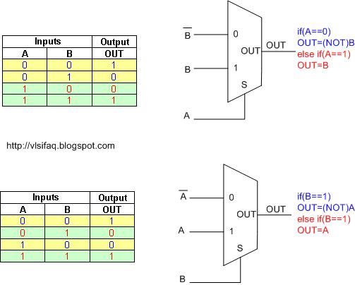
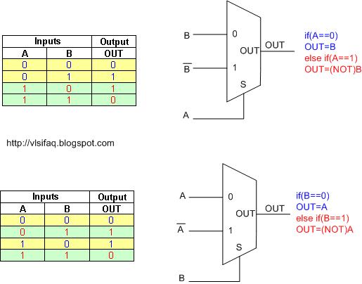
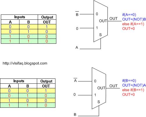
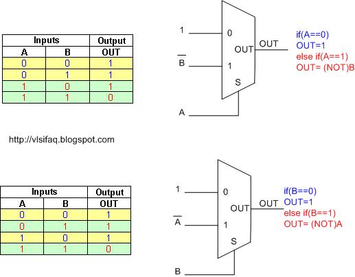
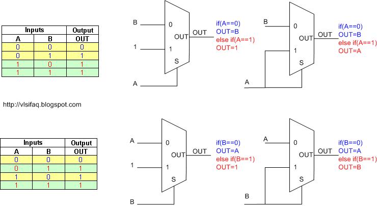
Draw OR gate using 2:1 MUX.
Applying similar concept of AND gate using 2:1 MUX, make either of input A or B as select line of MUX, connect other input to 0th input line. 1st input of the MUX is always tied to logic 1.
Related faq
AND gate using MUX
NAND gate using MUX
NOR gate using MUX
XOR gate using MUX
XNOR using MUX
How to get AND gate using 2:1 MUX?
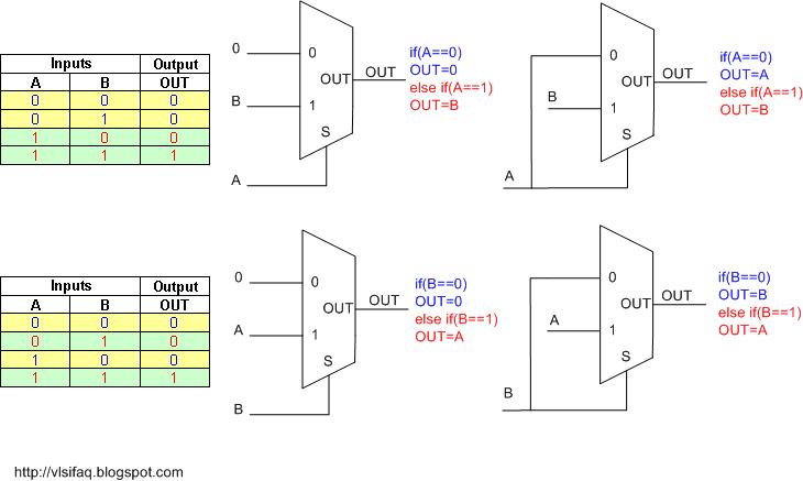
Look at the truth table of AND gate. When any of the one input is zero output is always zero (or same as that input); when the other input is one, output is dependent on the other input and is same as the other input. Using this property we can draw AND gate in four different ways using 2:1 MUX as shown in the above figure.
Similar concept can be applied to create all basic gates from 2:1 MUX. I will publish all these in coming blog posts along with the elaborated figures.
Related faq
OR gate using MUX
NAND gate using MUX
NOR gate using MUX
XOR gate using MUX
XNOR using MUX
FPGA Implementation of FIR Filter
FIR filters are most widely used in FPGA implementations owing to its linear phase property. Compared to IIR filters, FIR filters have simple and regular structures which are easy to implement on hardware. However FIR filters require higher number of taps compared to IIR filters to achieve the same frequency specification. FIR filter implementation on FPGA requires special attention as area, power; speed constraints have to be satisfied. A number of filter architectures for FPGA implementation have discussed. [1][2]. Out of these, Distributed Arithmetic (DA) architecture yields better area, power and speed trade off balance. [1]. A 7th order band pass filter is designed, simulated and synthesized. Modified DA architecture for the implementation of higher order filter is also discussed.
Design of filter using MATLAB
The filter specification is as follows:
Fpass1=1 KHz
Fstop1=0.9 KHz
Fpass2=2 KHz
Fstop2=2.1 KHz
pass band ripple=3dB
stop band ripple=60dB.
For this given specification 10 KHz of sampling frequency is chosen. Equiripple filter design method is opted. Equiripple method provides same tolerance as that of Kaiser Window with less number of filter orders. Filter is designed using ‘fdatool’ of the MATALAB software.
The magnitude and phase response of the designed filter is shown in Figure (1). The figure shows both reference filter response and response of the filter after coefficients have been quantized to fixed point representation. Order of the filter comes out to be 161 i.e. total 162 coefficients. Design of such a higher order filter is difficult task. Using ROM decomposition method of DA architecture we can reduce ROM size, however complexity of system design still exists. Hence to study DA architecture in FIR filter design a lower order filter is designed. Decrease in the order of the filter affects the frequency response of the filter, but it is time being neglected.
Figure (1) FIR band pass filter response
(click on the figure to enlarge)
Suitable architecture for filter implementation
There is much architecture available which implement FIR filter. Direct form of implementation of FIR filter suffers from less speed and more hardware resources. A single convolution operation requires around 20 CLBs in FPGA implementation. Thus implementation of 7 tap filter with input and coefficient as 8 bit width requires around 20x8=160 CLBs(~300 slices). Systolic array architecture even though improves timing by reducing critical path, utilizes same amount of hardware. When order of the filter increases hardware resource optimization becomes the real challenge. Distributed arithmetic (DA) architecture is comparatively more competitive to any of the other architectures in gate efficiency and operating speed.
Distributed Arithmetic
A brief theory of DA is explained below.
The convolution sum is given by y=f (h,y)=(from n=0 to N-1)∑h(n)*x(n). In DSP applications, if filter coefficients are known beforehand then partial products of the h (n).x (n) can be calculated. These partial products are stored in ROM as a look up table (LUT) and then accessed by the input samples each bits of which are used as the address for ROM. Coefficients h (n) are constants and inputs x (n) is a variable. Therefore x(n) can be represented as, x(n)=(from b=0 to B-1)∑xb(n).2b with xb(n)Є(0,1) where xb(n) denotes the bth of x(n) or nth sample of x.. The inner product y can be written as, y= (from n=0 to N-1) ∑h (n). (From b=0 to B-1) ∑ xb (k) .2b. redistributing the order of summation we get, y=(from b=0 to B-1) ∑ 2b*(from n=0 to N-1) ∑h(n).xb(n)=(from b=0 to B-1) ∑2b*(from n=0 to N-1) ∑f(h(n),xb(n)).
The distributed arithmetic requires 2N word LUT which is pre-programmed to the target device. These partial products are accessed using input vector xb= (xb(0), xb(1),…..xb(N-1)) are weighed by the power of 2 and accumulated. The inner product of y is computed after N look up cycles.
Figure (2) bit serial DA architecture [1]
(click on the figure to enlarge)
For signed DA system output y can be defined as, y=-2b.f(h(n).xb(n))+(from b=0 to B-1) ∑2b*(from n=0 to N-1) ∑f(h(n),xb(n)). The above equation can be implemented in two ways. In one method accumulator with add and subtract is used to add or subtract the partial products as per the sign bit. In another method ROM with an additional input is used. But this method puts burden of doubling the ROM size. [2]
Addressing of ROM can be either in bit serial or bit parallel fashion. Block diagram of bit serial architecture is shown in Figure (2). Bit serial (i.e. one bit per clock) architecture results in high gate efficiency while bit parallel (i.e. B bits per clock) architecture achieves higher speed. There is a performance price to be paid for this gate efficiency- the computation takes at least B clocks [1]. This can be observed in simulation diagram Figure (3).
Implementation
For the implementation of band pass filter as per the specification implementation of 161 order is necessary. Implementation of such a higher order using simple DA architecture requires ROM size of 2161 which is very large and practically not feasible to implement on FPGA. Even though it is possible to reduce the size of the ROM by utilizing symmetrical property of coefficients, ROM size of the present design is still very large. Hence a 7th order with 8 coefficients having 28=256 look up table values is implemented. Coefficients designed by the ‘fdatool’ of the MATLAB are:-0.027, -0.013, 0.004, 0.012, 0.012, 0.004, -0.013 and -0.027. These coefficients are scaled by 1000 to get integer values. Thus coefficient value becomes: -27, -13, 4, 12, 12, 4, -13 and -27. Distributed arithmetic look up table values (total 256 values) are generated by the executable program ‘dagen.exe’ provided with [2].
Total 8 inputs from ‘sample0’ to ‘sample7’ are given to filter. ‘en’ signal is used to indicate that the input supplied to filter are valid inputs. All the inputs are taken by the filter and stored in registers x0 to x7. These register values are used as ROM (or DA LUT) address vectors. For every partial accumulation bits in these registers are shifted using simple ‘for’ loop. DA LUT is written as separate module using ‘case’ statement and it is instantiated in main module ‘dasign’. This realizes into 256x8 sizes ROM. The signal ‘filt_out_valid’ is used to indicate that the available output is valid.
Simulation and Verification
Verification of the designed filter is carried out by testing impulse response and step response. Simulation waveform of the both step and impulse response is shown in Figure (3).
Impulse response
Impulse response of the system characterizes the filter. Impulse response of the filter is always equal to the value of the filter coefficients. Thus if designed filter produces the filter coefficients as its output for impulse input then correctness of the filter design is verified.
Designed filter is excited with impulse signal. The first sample is assigned a value of one (impulse signal) and all other inputs from sample1 to sample7 are made zero. When ‘en’ signal is enabled filter starts the processing of accumulation of partial products. After N clock cycles, where N is the order of the filter, first output is available and ‘filt_out_valid’ signal goes high indicating filter output is valid and can be read from the controlling hardware. This first output is equivalent to the first coefficient value -27. (Marked by circle in Figure (3)).
Figure (3) step and impulse response
(click on the figure to enlarge)
In next step impulse signal is shifted by one time unit i.e. ‘sample1’ is assigned a value of one and remaining all sample values are made zero. The corresponding obtained output is same as second coefficient value (-13). Similarly impulse signal is moved through all the input samples and corresponding outputs are observed. Simulation results clearly show all the coefficient values coming out as ‘filt_out’ as and when impulse signal traverses through input samples. Thus designed filter is verified by verifying the impulse response of the system.
Step response
Step response of the system also characterizes and verifies the functioning of the filter. For the step input filter output should be equal to the sum of all the coefficients. For our design expected step response output vale is=-27-13+4+12+12+4-13-27= -48.
The filter is excited with step input i.e. all input signals from ‘sample0’ to ‘sample7’ are assigned a value of one. When the signal ‘en’ is enabled after eight clock cycles ‘filt_out_valid’ signal goes high and valid output is available and equivalent to sum of coefficients. Thus step response of the filter is verified.
In simulation diagram shown in Figure (3), the value marked by the first circle is step response output and value marked by the second circle is the impulse response output i.e. first coefficient value. From the same simulation diagram it can be observed that total 7 clock cycles are required to calculate the output for every corresponding input. In systolic array architecture or direct method once the latency period is over or the processing pipeline full, for every clock pulse we get output. Thus in DA FIR filters extra hardware resources are required to control the filter.
FPGA Synthesis Results
The design is synthesized on the target device Spartan 3-3s200ft256-4. At first optimization goal is kept as speed. Then the number of slices used is 144 out of 1920(7%). Number of Slice Flip Flops used are125 out of 3840(3%). Number of 4 input LUTs are 261 out of 3840(6%). Total number of bonded IOBs used are 83 out of 173(47%).1 out of 8(12%) global clock is also used. As per timing analysis, maximum frequency of operation is 104.188 MHz.
The design is synthesized keeping optimization goal as area. Then, the devise utilization is as follows: the number of slices used is 171 out of 1920(8%). Number of slice flip flops used are93 out of 3840(2%). Number of 4 input LUTs are 205 out of 3840 (5%). Total numbers of bonded IOBs used are 83 out of 173(47%). One out of 8(12%) global clock is also used. As per timing analysis, maximum frequency of operation is 86.833 MHz.
References
[1]The Role of Distributed Arithmetic in FPGA-based Signal Processing , 5/6/2008
[2] U.Meyer-Baese, Digital signal processing with field programmable gate arrays, Springer, 2nd edition
[3] Stanley A. White Applications of Distributed Arithmetic to Digital Signal Processing: A Tutorial Review, IEEE ASSP magazine, July 1989
