The major design challenges of ASIC design consist of microscopic issues and macroscopic issues [1]. The microscopic issues are ultra-high speeds, power dissipation, supply rail drop, growing importance of interconnect, noise, crosstalk, reliability, manufacturability and the clock distribution. The macroscopic issues are time to market, design complexity, high levels of abstractions, reuse, IP portability, systems on a chip and tool interoperability.
To meet the design challenge of clock distribution, the timing analysis is performed. Timing analysis is to estimate when the output of a given circuit gets stable. Timing Analysis (TA) is a design automation program which provides an alternative to the hardware debugging of timing problems. The program establishes whether all paths within the design meet stated timing criteria, that is, that data signals arrive at storage elements early enough valid gating but not so early as to cause premature gating. The output of Timing Analysis includes ‘Slack” at each block to provide a measure of the severity of any timing problem [13].
Static vs. Dynamic Timing Analysis
Timing analysis can be
static or
dynamic.
Static Timing Analysis (STA) works with timing models where as the Dynamic Timing Analysis (DTA) works with spice models. STA has more pessimism and thus gives maximum delay of the design. DTA overcomes this difficulty because it performs full timing simulation. The problem associated with DTA is the computational complexity involved in finding the input pattern(s) that produces maximum delay at the output and hence it is slow. The static timing analyzer will report the following delays: Register to Register delays, Setup times of all external synchronous inputs, Clock to Output delays, Pin to Pin combinational delays. The clock to output delay is usually just reported as simply another pin-to-pin combinational delay. Timing analysis reports are often pessimistic since they use worst case conditions.
The wide spread use of STA can be attributed to several factors [2]:
The basic STA algorithm is linear in runtime with circuit size, allowing analysis of designs in excess of 10 million instances.
The basic STA analysis is conservative in the sense that it will over-estimate the delay of long paths in the circuit and under-estimate the delay of short paths in the circuit. This makes the analysis ”safe”, guaranteeing that the design will function at least as fast as predicted and will not suffer from hold-time violations.
The STA algorithms have become fairly mature, addressing critical timing issues such as interconnect analysis, accurate delay modeling, false or multi-cycle paths, etc.
Delay characterization for cell libraries is clearly defined, forms an effective interface between the foundry and the design team, and is readily available. In addition to this, the Static Timing Analysis (STA) does not require input vectors and has a runtime that is linear with the size of the circuit [9].
PVT vs. DelaySources of variation can be:
- Process variation (P)
- Supply voltage (V)
- Operating Temperature (T)
Process Variation [14]
This variation accounts for deviations in the semiconductor fabrication process. Usually process variation is treated as a percentage variation in the performance calculation. Variations in the process parameters can be impurity concentration densities, oxide thicknesses and diffusion depths. These are caused bye non uniform conditions during depositions and/or during diffusions of the impurities. This introduces variations in the sheet resistance and transistor parameters such as threshold voltage. Variations are in the dimensions of the devices, mainly resulting from the limited resolution of the photolithographic process. This causes (W/L) variations in MOS transistors.
Process variations are due to variations in the manufacture conditions such as temperature, pressure and dopant concentrations. The ICs are produced in lots of 50 to 200 wafers with approximately 100 dice per wafer. The electrical properties in different lots can be very different. There are also slighter differences in each lot, even in a single manufactured chip. There are variations in the process parameter throughout a whole chip. As a consequence, the transistors have different transistor lengths throughout the chip. This makes the propagation delay to be different everywhere in a chip, because a smaller transistor is faster and therefore the propagation delay is smaller.
Supply Voltage Variation [14]
The design’s supply voltage can vary from the established ideal value during day-to-day operation. Often a complex calculation (using a shift in threshold voltages) is employed, but a simple linear scaling factor is also used for logic-level performance calculations.
The saturation current of a cell depends on the power supply. The delay of a cell is dependent on the saturation current. In this way, the power supply inflects the propagation delay of a cell. Throughout a chip, the power supply is not constant and hence the propagation delay varies in a chip. The voltage drop is due to nonzero resistance in the supply wires. A higher voltage makes a cell faster and hence the propagation delay is reduced. The decrease is exponential for a wide voltage range. The self-inductance of a supply line contributes also to a voltage drop. For example, when a transistor is switching to high, it takes a current to charge up the output load. This time varying current (for a short period of time) causes an opposite self-induced electromotive force. The amplitude of the voltage drop is given by .V=L*dI/dt, where L is the self inductance and I is the current through the line.
Operating Temperature Variation [14]
Temperature variation is unavoidable in the everyday operation of a design. Effects on performance caused by temperature fluctuations are most often handled as linear scaling effects, but some submicron silicon processes require nonlinear calculations.
When a chip is operating, the temperature can vary throughout the chip. This is due to the power dissipation in the MOS-transistors. The power consumption is mainly due to switching, short-circuit and leakage power consumption. The average switching power dissipation (approximately given by Paverage = Cload*Vpower supply 2*fclock) is due to the required energy to charge up the parasitic and load capacitances. The short-circuit power dissipation is due to the finite rise and fall times. The nMOS and pMOS transistors may conduct for a short time during switching, forming a direct current from the power supply to the ground. The leakage power consumption is due to the nonzero reverse leakage and sub-threshold currents. The biggest contribution to the power consumption is the switching. The dissipated power will increase the surrounding temperature. The electron and hole mobility depend on the temperature. The mobility (in Si) decreases with increased temperature for temperatures above –50 °C. The temperature, when the mobility starts to decrease, depends on the doping concentration. A starting temperature at –50 °C is true for doping concentrations below 1019 atoms/cm3. For higher doping concentrations, the starting temperature is higher. When the electrons and holes move slower, then the propagation delay increases. Hence, the propagation delay increases with increased temperature. There is also a temperature effect, which has not been considered. The threshold voltage of a transistor depends on the temperature. A higher temperature will decrease the threshold voltage. A lower threshold voltage means a higher current and therefore a better delay performance. This effect depends extremely on power supply, threshold voltage, load and input slope of a cell. There is a competition between the two effects and generally the mobility effect wins.
The following figure shows the PVT operating conditions.

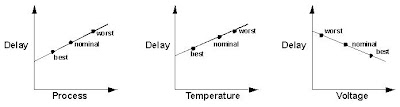
The best and worst design corners are defined as follows:
- Best case: fast process, highest voltage and lowest temperature
- Worst case: slow process, lowest voltage and highest temperature
On Chip Variation
On-chip variation is minor differences on different parts of the chip within one operating condition. On-Chip variation (OCV) delays vary across a single die due to:
- Variations in the manufacturing process (P)
- Variations in the voltage (due to IR drop)
- Variations in the temperature (due to local hot spots etc)
This need is to be modeled by scaling the coefficients. Delays have uncertainty due to the variation of Process (P), Voltage (V), and Temperature (T) across large dies. On-Chip variation allows you to account for the delay variations due to PVT changes across the die, providing more accurate delay estimates.
Timing Analysis With On-Chip Variation- For cell delays, the on-chip variation is between 5 percent above and 10 percent below the SDF back-annotated values.
- For net delays, the on-chip variation is between 2 percent above and 4 percent below the SDF back-annotated values.
- For cell timing checks, the on-chip variation is 10 percent above the SDF values for setup checks and 20 percent below the SDF values for hold checks.
In Prime Time, OCV derations are implemented using the following commands:
- pt_shell> read_sdf -analysis_type on_chip_variation my_design.sdf
- pt_shell> set_timing_derate -cell_delay -min 0.90 -max 1.05
- pt_shell> set_timing_derate -net -min 0.96 -max 1.02
- pt_shell> set_timing_derate -cell_check -min 0.80 -max 1.10
In the traditional deterministic STA (DSTA), process variation is modeled by running the analysis multiple times, each at a different process condition. For each process condition, a so-called corner file is created that specifies the delay of the gates at that process condition. By analyzing a sufficient number of process conditions, the delay of the circuit under process variation can be bounded.
The uncertainty in the timing estimate of a design can be classified into three main categories.
- Modeling and analysis errors: Inaccuracy in device models, in the extraction and reduction of interconnect parasitics and in the timing analysis algorithms.
- Manufacturing variations: Uncertainty in the parameters of a fabricated devices and interconnects from die-to-die and within a particular die.
- Operating context variations: Uncertainty in the operating environment of a particular device during its lifetime, such as temperature, supply voltage, mode of operation and lifetime wear-out.
For instance, the STA tool might utilize a conservative delay noise algorithm resulting in certain paths operating faster than expected. Environmental uncertainty and uncertainty due to modeling and analysis errors are typically modeled using worst-case margins, whereas uncertainty in process is generally treated statistically.
Taxonomy of Process VariationsAs process geometries continue to shrink, the ability to control critical device parameters is becoming increasingly difficult and significant variations in device length, doping concentrations and oxide thicknesses have resulted [9]. These process variations pose a significant problem for timing yield prediction and require that static timing analysis models the circuit delay not as a deterministic value, but as a random variable.
Process variations can either systematic or random.
- Systematic variation: Systematic variations are deterministic in nature and are caused by the structure of a particular gate and its topological environment. The systematic variations are the component of variation that can be attributed to a layout or manufacturing equipment related effects. They generally show spatial correlation behavior.
- Random variation: Random or non-systematic variations are unpredictable in nature and include random variations in the device length, discrete doping fluctuations and oxide thickness variations. Random variations cannot be attributed to a specific repeatable governing principle. The radius of this variation is comparable to the sizes of individual devices, so each device can vary independently.
Process variations can classified as follow:
- Inter-die variation or die-to-die: Inter-chip variations are variations that occur from one die to next, meaning that the same device on a chip has different features among different die of one wafer, from wafer to wafer and from wafer lot to wafer lot. Die-to-die variations have a variation radius larger than the die size including within wafer, wafer to wafer, lot to lot and fab to fab variations [12].
- Intra-die or within-die variation: Intra-die variations are the variations in device features that are present within a single chip, meaning that a device feature varies between different locations on the same die. Intra-chip variations exhibit spatial correlations and structural correlations.
- Front-end variation: Front-end variations mainly refer to the variations present at the transistor level. The primary components of the front end variations entail transistor gate length and gate width, gate oxide thickness, and doping related variations. These physical variations cause changes in the electrical characteristics of the transistors which eventually lead to the variability in the circuit performance.
- Back-end variation: Back-end variations refer to the variations on various levels of interconnecting metal and dielectric layers used to connect numerous devices to form the required logic gates.
In practice, device features vary among the devices on a chip and the likelihood that all devices have a worst-case feature is extremely small. With increasing awareness of process variation, a number of techniques have been developed which model random delay variations and perform STA. These can be classified into f
ull-chip analysis and
path-based analysis approaches.
Full Chip AnalysisFull-chip analysis models the delay of a circuit as a random variable and endeavors to compute its probability distribution. The proposed methods are heuristic in nature and have a very high worst-case computational complexity. They are also based on very simple delay models, where the dependence of gate delay due to slope variation at the input of the gate and load variation at the output of the gate is not modeled. When run time and accuracy are considered, full chip STA is not yet practical for industrial designs.
Path Based STAPath based STA provides statistical information on a path-by-path basis. It accounts for intra-die process variations and hence eliminates the pessimism in deterministic timing analysis, based on case files. It is a more accurate measure of which paths are critical under process variability, allowing more correct optimization of the circuit. This approach does not include the load dependence of the gate delay due to variability of fan out gates and does not address spatial correlations of intra-die variability.
To compute the intra-die path delay component of process variability, first the sensitivity of gate delay, output slope and input load with respect to slope, output load and device length are computed. Finally, when considering sequential circuits, the delay variation in the buffered clock tree must be considered.
In general, the fully correlated assumptions will under-estimate the variation in the arrival times at the leaf nodes of the clock tree which will tend to overestimate circuit performance.
References[1]
http://www.ecs.umass.edu/ece/vspgroup/burleson/courses/558/558%20L01.pdf[2] David Blaauw, Kaviraj Chopra, Ashish Srivastava and Lou Scheffer, “Statistical Timing Analysis: From basic principles to state-of-the-art.” Transactions on Computer-Aided Design of Integrated Circuits and Systems (T-CAD), invited review article, to appear.
[3] Andrew B. Kahng, Bao Liu and Xu Xu, “Statistical Timing Analysis in the Presence of Signal-Integrity Effects,” IEEE Transactions on Computer-Aided Design of Integrated Circuits and Systems, vol. 22, no.10, Oct. 2007.
[4]
http://eetimes.com/news/design/showArticle.jhtml?articleID=163703301[5] Jinjun Xiong, Vladimir Zolotov, Natesan Venkateswaran and Chandu Visweswariah, “Criticality Computation in Parameterized Statistical Timing,” DAC 2006: 63-68.
[6]
http://www.cdnusers.org/Interviewsstastratosphere/tabid/418/Default.aspx[7]
http://www.edadesignline.com/showArticle.jhtml;jsessionid=1ISIZARO0KMGMQSNDLOSKH0CJUNN2J[8] A. Nardi, E. Tuncer, S. Naidu, A. Antonau, S. Gradinaru, T.Lin and J. Song, “Use of Statistical timing Analysis on Real Designs” Proceedings of the IEEE Design, Automation & Test in Europe Conference & Exhibition, pp. 1-6, April 2007.
[9] Agarwal, A. Blaauw, D. Zolotov, V. Sundareswaran, S. Min Zhao Gala, K. and Panda, R., “Statistically Delay computation considering spatial correlations,” Proceedings of the ASP-DAC 2003, pp.271-276, Jan 2003.
[10] Aseem Agarwal, David Blaauw and Vladimir Zolotov, “Statistical Timing Analysis for Intra-Die process Variations with spatial correlations” IEEE Transactions on Computer-Aided Design, pp. 900-907, Nov 2003.
[11] Aseem Agarwal, David Blaauw and Vladimir Zolotov, “Statistical Clock Skew Analysis Considering Intra-Die Process Variations,” IEEE Transactions on Computer-Aided Design, vol. 23, no. 8, pp. 1231-1242, Aug, 2004.
[12] Ayhan Mutlu, Kelvin J. Le, Mustafa Celik, Dar-sun Tsien, Garry Shyu, and Long-Ching Yeh, “An Exploratory Study on Statistical Timing Analysis and Parametric Yield Optimization,” Proceedings of the 8th International Symposium on Quality Electronic Design, pp. 677-684, 2007.
[13] Robert B.Hitchcock, Sr, Gordon L. Smith, David D. Cheng, “Timing Analysis of Computer Hardware,” IBM Journal, vol. 26, no. 1, Jan 1981.
Below link in contributed by Rajneesh. Thanks Raj.
(14) "Investigation of typical 0.13 μm CMOS technology timing effects in a complex digital system on-chip",
www.diva-portal.org/diva/getDocument?urn_nbn_se_liu_diva-2118-1__fulltext.pdfAuthors1)Sowmya yadala, MS in VLSI System Design from
MSRSAS, Bangalore. She can be reached at:
sowmyayadala@gmail.com2) Myself !


