Universal Asynchronous Receiver/Transmitter - UART-RS232


The Universal Asynchronous Receiver/Transmitter (UART) controller is the key component of the serial communications subsystem of a microprocessors, microcontrollers and computers. The UART can take bytes of data in parallel fashion and transmits the individual bits in a sequential fashion. At the same time, a second UART can receive serial bits sent by UART and convert the bits into complete bytes. There are two types of serial transmission: Synchronous and Asynchronous. The asynchronous communication is known as UART and asynchronous is known as Universal Synchronous-Asynchronous Receiver/Transmitter (USART). Latest standard UART employ FIFO buffer for improved functional capability. UARTs are generally used to modem control functions. Hence they have several functional control registers using which efficient interface can be established with host processor. Embedded processors employ built in hard core UART block while soft IP UART provide programmable and reconfigurable flexibilities which are very much advantages in FPGA applications. Hardware Descriptive Languages (HDL) like verilog can be used for the behavioral description of the UART.

The UART device changes incoming parallel data to serial data which can be sent on a communication line. A second UART is used to receive the information which converts serial data to parallel. The UART performs all the tasks, timing, parity checking, etc. needed for the communication. The UART requires external line drivers (EIA RS 232 C interface) to interface to external world. In computer systems, the UART is connected to circuitry that generates signals that comply with the EIA RS232-C specification. There is also a CCITT standard named V.24 that resembles the specifications included in RS232-C. Registers are accessible to set or review the communication parameters to use the UART in different environments. Using these registers the communication speed (baud rate), the type of parity check, and the way incoming information is signaled to the running software are set according to the requirement of host processor.

Serial UART types

PC compatible serial communication started with the 8250 UART in the IBM XT machines. Then UART is upgraded to 8250A, 8250B and then 16450 (manufactured by National Semiconductor) which is implemented in the AT machines. The higher bus speed could not be reached by the 8250 series but newer 16450 were capable of handling a communication speed of 38.4 kbs. 16450 had 1 byte FIFO. The later improved version 16550A contained two on-board FIFO buffers, each capable of storing 16 bytes. One buffer for transmitter and one buffer for receiver. This made it possible to increase maximum reliable communication speeds to 115.2 kbs and use effectively in modems with on-board compression. DMA access ability is provided in 16550. Two pins were redefined for this purpose. DMA transfer is not used with most applications. The most common UART used is 16550A. Newer versions such as 16650 contain two 32 byte FIFO's and on board support for software flow control are latest advancements in industry. Texas Instruments is developing the 16750 which contains 64 byte FIFO's.

A UART usually contains the following components:

  • Baudrate clock generator: Multiple of the bit rate to improve sampling in the middle of a bit period. For generating this timing information, each UART uses an oscillator generating a frequency of about 1.8432 MHz. This frequency is divided by 16 to generate the time base for communication. Hence the maximum allowed communication speed is 115200 bps. UARTs like the 16550 are capable of handling higher input frequencies up to 24 MHz which makes it possible to communicate with a maximum speed of 1.5 Mbps.
  • Input and output shift registers: Each UART contains a shift register which is the fundamental method of conversion between serial and parallel forms. These registers shifts the data that has to be serially transmitted or serially received.
  • Transmit and receive control: This control logic checks for the control signals from host processor to start or stop the transmission and reception of the data bits. In case of any error it also generates error signals.
  • Optional transmit and receive buffers: Buffers can be used to hold the data temporarily.
  • Optional parallel data bus buffer: This buffer improves the speed.
  • Optional FIFO: The UART works by writing data from the host processor to its FIFO buffers, and feeding the data from the buffer to the serial device in the format dictated by the user (typically 8-N-1).


Serial Data Format and Asynchronous Serial Transmission

As the name indicates, asynchronous transmission need not send clock signal to send the data to the receiver. The sender and receiver must agree on timing parameters in advance and special bits such as start and stop bits are added to each word which is used to synchronize the sending and receiving units. The UART serial data format is shown in Figure (1).


Figure (1) Serial Data Format

A bit called the "Start Bit" is added to the beginning of each word that is to be transmitted. The Start Bit indicates the start of the data transmission and it alerts the receiver that a word of data is about to be sent. Upon reception of start bit the clock in the receiver goes into synchronization with the clock in the transmitter. The accuracy of these two clocks should not deviate more than 10% during the transmission of the remaining bits in the word.

The individual bits of the word of data are sent after the start bit. Least Significant Bit (LSB) is sent first. The transmitter does not know when the receiver has read at the value of the bit. The transmitter begins transmitting the next bit of the word on next clock edge.

Parity bit is be added when the entire data word has been sent. This bit can be used to detect errors at the receiver side. Then one Stop Bit is sent by the transmitter to indicate the end of the valid data bits.

On the receiver side once it receives all of the bits in the data word, it can check for the Parity Bits. To accomplish this task both transmitter and receiver must agree on whether a Parity Bit is to be used. Then Stop Bit is encountered by receiver. A missing stop bit may result entire data to be garbage. This will cause a Framing Error and will be reported to the host processor when the data word is read. Framing Error can be caused due to mismatch of transmitter and receiver clocks.

The UART automatically discards the Start, Parity and Stop bits irrespective of whether data is received correctly or not. If the sender and receiver are configured identically, these bits are not passed to the host. To transmit new word, the Start Bit for the new word is sent as soon as the Stop Bit for the previous word has been sent.

The transmission speed in asynchronous communication is measured by Baud Rate. A Baud Rate represents the number of bits that are actually being sent over the media. The Baud rate includes the Start, Stop and Parity bits. The Bit rate (Bits per Second-bps) represents the amount of data that is actually sent from the transmitting device to the other device. Speeds for UARTs are in bits per second (bit/s or bps), although often incorrectly called the baud rate. Standard baud rates are: 110, 300, 1200, 2400, 4800, 9600, 14400, 19200, 28800, 38400, 57600, 76800, 115200, 230400, 460800, 921600, 1382400, 1843200 and 2764800 bit/s.


UART Registers

Twelve registers control the communication between the processor and the UART. Behavior of the communication can be changed by reading or writing registers. Each register is eight bits wide. On PC compatible devices, the registers are accessible in the I/O address area. The function of each register is discussed here in brief. The registers are shown in Figure


Figure (2) The 16550 UART registers

RBR: Receiver buffer register

The Receiver Buffer Register (RBR) contains the byte received if no FIFO is used, or the oldest unread byte with FIFO's. If FIFO buffering is used, each new read action of the register will return the next byte, until no more bytes are present. Bit 0 in the Line Status Register (LSR) can be used to check if all received bytes have been read. This bit will change to zero if no more bytes are present.

THR: Transmitter holding register

Transmitter Holding Register (THR) is used to buffer outgoing characters. Without FIFO buffering, only one character can be stored. Otherwise the amount of characters depends on the type of UART. To check if new information must be written to THR Bit 5 in the Line Status Register (LSR) can be used. Empty register is indicated by the value 1. If FIFO buffering is used, more than one character can be written to the transmitter holding register when the FIFO is empty.

IER: Interrupt enable register

In interrupt driven configuration, the UART will signal each change by generating a processor interrupt. A software routine must be read interrupt signal to handle the interrupt and to check what state change was responsible for it. Interrupt enable register (IER) is used to enable the interrupt.

IIR: Interrupt identification register

The Interrupt Identification Register (IIR) bits show the current state of the UART and which state change caused the interrupt to occur. Based on bit values of the IIR interrupt can be serviced.

FCR: FIFO control register

The FIFO control register (FCR) is present starting with the 16550 series. The behavior of the FIFOs in the UART is controlled by this register. If a logical value 1 is written to bits 1 or 2, the function attached is triggered. The other bits are used to select a specific FIFO mode.

LCR: Line control register

The Line Control Register (LCR) is used at initialization to set the communication parameters such as parity, number of data bits etc. The register also controls the accessibility of the DLL and DLM registers.

MCR: Modem control register

Handshaking actions with the attached device are accomplished by the Modem Control Register (MCR). In the UART series 16550, setting and resetting of the control signals must be done by software. But in the new 16750, flow control automatically handled.

LSR: Line status register

The Line Status Register (LSR) shows the current state of communication. Errors, the state of the receiver and transmit buffers are available.

MSR: Modem status register

The Modem Status Register (MSR) contains information about the four incoming modem control lines on the device. The four most significant bits contain information about the current state of the inputs. The least four significant bits are used to indicate state changes. Each time the register is read the four LSB's are reset.

DLL and DLM: Divisor latch registers

The communication speed of the UART is changed by using a programmable value stored in Divisor Latch Registers DLL and DLM which contains the least and most significant registers.


UART Transmitter

The block representation of serial data transmission is depicted in Figure (3).The serial transmit block has FIFO buffer into which data is written by the host processor. After the data is written into the buffers it is transmitted serially onto tx. As long as the FIFO is not full the serial transmit block sets the signal tx_en high.


Figure (3) Serial data transmission


Transmit FIFO

The FIFO is 8-bit by 32-word. It receives control signals from the serial transmit block. The data on signal data_bus is written into its buffer. At the same time the write pointer is incremented. The data is read onto FIFO and the read pointer is reset when the read pointer has reached its maximum. The write pointer is cleared when the write pointer has reached its maximum. The tx_en is set low when the FIFO is full.

Serial Transmit Block

This component is responsible for serial transmission of data onto tx. It generates the requisite control signals for reading and writing the transmit FIFO. This signal is used as an enable by the transmit data counter, and the transmit block. The transmit data counter keeps count of the number of data bits transmitted onto tx. These signals are provided by the transmit control block. The parity counter counts the number of bits that were high in the eight bits of data being transmitted. The transmit control block controls the whole process of transmission. It is modeled in the form of a state machine.


UART-Receiver

The block representation of serial data reception is depicted in Figure (4).The serial receive block can also has a FIFO buffers. The block checks for the parity and the validity of the data frame on the rx input and then writes correct data into its buffers. It also sets the signal byte_ready low if its FIFO is empty.

Receive FIFO

The FIFO is 8-bit wide and 32 byte deep. It receives control signals from the serial receive block. The data received from the receive block written into its buffer. The write pointer is cleared when the write pointer reaches its maximum limit before further increment.


Figure (4) Serial data reception

Serial Receive Block

Serial data is received by this component. It generates the requisite control signals for reading and writing the receive FIFO. It generates required sample clock to sample the incoming data and determine the baud rate of the incoming data.


UART Errors

Overrun Error

An "overrun error" occurs when the UART cannot process the byte that just came in before the next one arrives. The host processor must service the UART in order to remove characters from the buffer. If the host processor does not service the UART and the buffer becomes full, then Overrun Error will occur.

Framing Error

A "Framing Error" occurs when the designated "start" and "stop" bits are not valid. Start bit acts as a reference for the remaining bits. When the "stop" bit is expected if the data line is not in the expected idle state a Framing Error will occur.

Parity Error

A "Parity Error" occurs when the number of "active" bits does not agree with the specified parity configuration of the UART.


External Interface

The external signalling levels that are used between different equipment are not generated by UART. An interface is used to convert the logic level signals of the UART to the external signalling levels. Examples of standards for voltage signalling are RS-232, RS-422 and RS-485 from the EIA. For embedded system applications UARTs are commonly used with RS-232. It is useful to communicate between microcontrollers and also with PCs. MAX 232 is one of the example ICs which provide RS232 level signals.
Asynchronous FIFO: Simulation and Synthesis


Asynchronous FIFO: Simulation using Modelsim

Note: Diagram numbers are continued from the previous post.

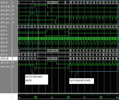
Test bench strategy is to generate all corner conditions like full and empty. Simulation waveforms are shown in Figure (11) to Figure (13). These waveforms are generated using test bench program provided in previous article. Read clock frequency 50 MHz and write clock frequency 10 MHz are generated using initial procedural statements:

initial begin #10 r_clk=0; forever #10 r_clk=~r_clk; end

initial begin #5 w_clk=0; forever #50 w_clk=~w_clk; end

Duty cycle of r_clk is 10 nS and w_clk is 50 nS.

Other conditions like w_en, r_en etc are generated using below set of statements:

initial begin d_in=1;

@(posedge w_en);

repeat(20) @(posedge w_clk) d_in=d_in+2;

repeat(20) @(posedge w_clk) d_in=d_in-1;

end

initial begin reset=1;#30 reset=0;end

initial begin fork #50 w_en=1; #1800 w_en=0; #2500 w_en=1 ; join end

initial begin fork #50 r_en=0; #1850 r_en=1; #2400 r_en=0; #2500 r_en=1; join end

In the above two statements ‘fork’ and ‘join’ are used to start the simulation at zero simulation time. Reset signal is activated for first 30 nS and then it is deactivated. For the first 5 nS reset is active which tests asynchronous reset condition

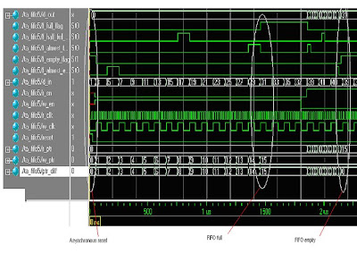
For asynchronous reset condition except d_out all other variables are initialized to default states, including f_empty_flag. r_ptr, w_ptr, ptr_diff are initialized to zero. All FIFO status flags are initialized to default values. Since reset signal is connected to binary counters, reset of counters causes reset of both read and write pointers, pointer difference and all status flags. This can be observed in the simulated waveform shown in Figure (11). Verilog code has to be improved for the complete asynchronous reset including reset of d_out. When I tried to add asynchronous reset to RTL code of dual port RAM, synthesizer does not infer dual port RAM. Instead, it infers set of registers. This problem has to be sorted out.


Figure (11) Simulation waveform 1


After 1800nS amount of time w_en is disabled. This time gap is chosen so that FIFO full condition can be generated. (See Figure (11)). When ptr_diff becomes equal to (fifo_depth-1) f_full_flag goes high and w_ptr stops counting. Further data on the d_in bus will overwrite on the last location of the FIFO. This is unavoidable since there is no control over the d_in bus. When FIFO is half filled (i.e. fifo_depth/2) f_half_full_flag is asserted and in next w_clk cycle it goes to normal state. Similarly when FIFO reaches almost full condition f_almost_full_flag is asserted. Thus all status flags are activated within zero clock delay. (See Figure (13))

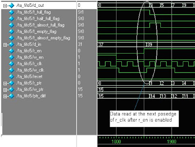
Signal r_en enabled to start read operation. At this time w_en is disabled so that empty condition can be generated. R_en is detected in coming positive edge of clock cycle and hence data is read with zero r_clk cycle delay. (See Figure (12). When ptr_diff becomes zero f_empty_flag is asserted. r_ptr stops incrementing. But for every r_clk data is read from the last location and put on to the d_out bus.


Figure (12) Simulation waveform 2


When both r_en and w_en are enabled read clock domain has to wait till data has been written to FIFO. Thus empty flag goes low for the positive edge of w_clk. At the next positive edge of the r_clk data has been read out and put in d_out bus. Since r_ptr has incremented ptr_diff becomes zero and f_empty_flag goes high again. This status remains till next positive edge of w_clk. Observe the asynchronous read and write operation in the Figure (13). F_empty_flag and r_next_en signals are compliment to each other. As soon as data is written to the FIFO r_next_en signal is enabled. Read address is incremented and both read and write pointers become equal. This makes the ptr_diff zero and once again f_empty_flag is asserted. Thus there is no pessimistic reporting of assertion or removal of FIFO status flags.


Thus overall performance of the designed FIFO resembles the performance of the FIFO IP core provided by the Xilinx. Algorithm and methodology used are entirely different in both designs. IP core uses acknowledgement signal for the confirmation of read and write operation. But proposed design does not have any such mechanism. It is assumed that data sending and receiving hardware takes care of the data once the FIFO full and empty condition are asserted.


Figure (13) Simulation waveform 3


Asynchronous FIFO: Synthesis using Xilinx ISE and Spartan 3


Synthesis of the design based on two different optimization goal makes difference in usage of logic cells and maximum operating frequency of the design. Maintaining ‘speed’ as optimization goal, maximum achievable frequency is 113.830MHz.

----------------------------------------------

Timing Summary:

Speed Grade: -5

Minimum period: 8.785ns (Maximum Frequency: 113.830MHz)

Minimum input arrival time before clock: 4.692ns

Maximum output required time after clock: 12.049ns

Maximum combinational path delay: No path found

---------------------------------------------------------


Maintaining ‘area’ as optimization goal, maximum achievable frequency is 90.212MHz.


--------------------------------------------------------

Timing Summary:

Speed Grade: -5

Minimum period: 11.085ns (Maximum Frequency: 90.212MHz)

Minimum input arrival time before clock: 4.574ns

Maximum output required time after clock: 13.375ns

Maximum combinational path delay: No path found

---------------------------------------------------------------------


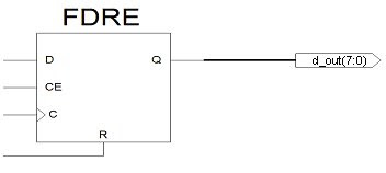
The difference in the operating frequency can be attributed to the delay in the adder-subtractor circuit. Dual port distributed RAM is used for memory. Output data d_out is registered (RTL schematic is shown in Figure (14)) which is one of the advantages of this design.


Figure (14) Registered output


The part of the synthesis report generated by Xilinx ISE, shown below infers the hardware which remains same for both optimization goals.


----------------------------------------------------------------------

Synthesizing Unit .

Related source file is a_fifo5.v.

Found 16x8-bit dual-port distributed RAM for signal .

-----------------------------------------------------------------------

| aspect ratio | 16-word x 8-bit | |

| clock | connected to signal | rise |

| write enable | connected to internal node | high |

| address | connected to signal | |

| dual address | connected to signal | |

| data in | connected to signal | |

| data out | not connected | |

| dual data out | connected to internal node | |

| ram_style | Auto | |

-----------------------------------------------------------------------

INFO:Xst:1442 - HDL ADVISOR - The RAM contents appears to be read asynchronously. A synchronous read would allow you to take advantage of available block RAM resources, for optimized device usage and improved timings. Please refer to your documentation for coding guidelines.

Found 8-bit register for signal .

Found 4-bit addsub for signal <$n0003>.

Found 4-bit comparator greater for signal <$n0007> created at line 60.

Found 4-bit comparator less for signal <$n0008> created at line 62.

Found 4-bit adder for signal <$n0009> created at line 64.

Found 4 1-bit 2-to-1 multiplexers.

Summary:

inferred 1 RAM(s).

inferred 8 D-type flip-flop(s).

inferred 2 Adder/Subtracter(s).

inferred 2 Comparator(s).

inferred 4 Multiplexer(s).

Unit synthesized.

-----------------------------------------------------------------


But observation of the low level synthesis gives the device utilization summary. Device utilization with ‘speed’ as optimization goal is as follows:


-----------------------------------------

Device utilization summary:

---------------------------

Selected Device: 3s200ft256-5

Number of Slices: 36 out of 1920 1%

Number of Slice Flip Flops: 20 out of 3840 0%

Number of 4 input LUTs: 50 out of 3840 1%

Number of bonded IOBs: 24 out of 173 13%

Number of GCLKs: 2 out of 8 25%

-------------------------------------------------------------


Device utilization with ‘area’ as optimization goal is as follows:


-----------------------------------------

Device utilization summary:

-----------------------------------------

Selected Device : 3s200ft256-5

Number of Slices: 34 out of 1920 1%

Number of Slice Flip Flops: 16 out of 3840 0%

Number of 4 input LUTs: 47 out of 3840 1%

Number of bonded IOBs: 24 out of 173 13%

Number of GCLKs: 2 out of 8 25%

------------------------------------------------------------


In the case of ‘area’, slices are reduced by 2, slice flip-flops are reduced by 4, 4 input LUTs are reduced by 3. For the present design read clock is working at 50MHz. Hence operating speed of the design is very important and optimization goal is maintained as ‘speed’. Other than the package pin constraints, area constraints or timing constraints are not provided to the design while synthesis. Since the design doesn’t consume much of the resource of the FPGA area is not important factor. Package pin constraints are given so as to implement the design on Spartan 3 development board. This is done for the fifo_top.v code which includes clock generation code for the design.


Related Articles


What are the different types of delays in ASIC or VLSI design?

Different Types of Delays in ASIC or VLSI design
  • Source Delay/Latency
  • Network Delay/Latency
  • Insertion Delay
  • Transition Delay/Slew: Rise time, fall time
  • Path Delay
  • Net delay, wire delay, interconnect delay
  • Propagation Delay
  • Phase Delay
  • Cell Delay
  • Intrinsic Delay
  • Extrinsic Delay
  • Input Delay
  • Output Delay
  • Exit Delay
  • Latency (Pre/post CTS)
  • Uncertainty (Pre/Post CTS)
  • Unateness: Positive unateness, negative unateness
  • Jitter: PLL jitter, clock jitter

Gate delay
  • Transistors within a gate take a finite time to switch. This means that a change on the input of a gate takes a finite time to cause a change on the output.[Magma]

  • Gate delay =function of(i/p transition time, Cnet+Cpin).
  • Cell delay is also same as Gate delay.

Source Delay (or Source Latency)
  • It is known as source latency also. It is defined as "the delay from the clock origin point to the clock definition point in the design".

  • Delay from clock source to beginning of clock tree (i.e. clock definition point).
  • The time a clock signal takes to propagate from its ideal waveform origin point to the clock definition point in the design.

Network Delay(latency)
  • It is also known as Insertion delay or Network latency. It is defined as "the delay from the clock definition point to the clock pin of the register".
  • The time clock signal (rise or fall) takes to propagate from the clock definition point to a register clock pin.

Insertion delay
  • The delay from the clock definition point to the clock pin of the register.

Transition delay
  • It is also known as "Slew". It is defined as the time taken to change the state of the signal. Time taken for the transition from logic 0 to logic 1 and vice versa . or Time taken by the input signal to rise from 10%(20%) to the 90%(80%) and vice versa.
  • Transition is the time it takes for the pin to change state.

Slew
  • Rate of change of logic.See Transition delay.
  • Slew rate is the speed of transition measured in volt / ns.

Rise Time

  • Rise time is the difference between the time when the signal crosses a low threshold to the time when the signal crosses the high threshold. It can be absolute or percent.
  • Low and high thresholds are fixed voltage levels around the mid voltage level or it can be either 10% and 90% respectively or 20% and 80% respectively. The percent levels are converted to absolute voltage levels at the time of measurement by calculating percentages from the difference between the starting voltage level and the final settled voltage level.

Fall Time


  • Fall time is the difference between the time when the signal crosses a high threshold to the time when the signal crosses the low threshold.
  • The low and high thresholds are fixed voltage levels around the mid voltage level or it can be either 10% and 90% respectively or 20% and 80% respectively. The percent levels are converted to absolute voltage levels at the time of measurement by calculating percentages from the difference between the starting voltage level and the final settled voltage level.
  • For an ideal square wave with 50% duty cycle, the rise time will be 0.For a symmetric triangular wave, this is reduced to just 50%.


  • The rise/fall definition is set on the meter to 10% and 90% based on the linear power in Watts. These points translate into the -10 dB and -0.5 dB points in log mode (10 log 0.1) and (10 log 0.9). The rise/fall time values of 10% and 90% are calculated based on an algorithm, which looks at the mean power above and below the 50% points of the rise/fall times. Click here to see more.

Path delay
  • Path delay is also known as pin to pin delay. It is the delay from the input pin of the cell to the output pin of the cell.

Net Delay (or wire delay)
  • The difference between the time a signal is first applied to the net and the time it reaches other devices connected to that net.
  • It is due to the finite resistance and capacitance of the net.It is also known as wire delay.
  • Wire delay =fn(Rnet , Cnet+Cpin)
Propagation delay
  • For any gate it is measured between 50% of input transition to the corresponding 50% of output transition.
  • This is the time required for a signal to propagate through a gate or net. For gates it is the time it takes for a event at the gate input to affect the gate output.
  • For net it is the delay between the time a signal is first applied to the net and the time it reaches other devices connected to that net.

  • It is taken as the average of rise time and fall time i.e. Tpd= (Tphl+Tplh)/2.


Phase delay
  • Same as insertion delay

Cell delay
  • For any gate it is measured between 50% of input transition to the corresponding 50% of output transition.

Intrinsic delay
  • Intrinsic delay is the delay internal to the gate. Input pin of the cell to output pin of the cell.
  • It is defined as the delay between an input and output pair of a cell, when a near zero slew is applied to the input pin and the output does not see any load condition.It is predominantly caused by the internal capacitance associated with its transistor.
  • This delay is largely independent of the size of the transistors forming the gate because increasing size of transistors increase internal capacitors.


Extrinsic delay
  • Same as wire delay, net delay, interconnect delay, flight time.
  • Extrinsic delay is the delay effect that associated to with interconnect. output pin of the cell to the input pin of the next cell.

Input delay
  • Input delay is the time at which the data arrives at the input pin of the block from external circuit with respect to reference clock.

Output delay
  • Output delay is time required by the external circuit before which the data has to arrive at the output pin of the block with respect to reference clock.

Exit delay
  • It is defined as the delay in the longest path (critical path) between clock pad input and an output. It determines the maximum operating frequency of the design.

Latency (pre/post cts)
  • Latency is the summation of the Source latency and the Network latency. Pre CTS estimated latency will be considered during the synthesis and after CTS propagated latency is considered.

Uncertainty (pre/post cts)
  • Uncertainty is the amount of skew and the variation in the arrival clock edge. Pre CTS uncertainty is clock skew and clock Jitter. After CTS we can have some margin of skew + Jitter.

Unateness
  • A function is said to be unate if the rise transition on the positive unate input variable causes the ouput to rise or no change and vice versa.
  • Negative unateness means cell output logic is inverted version of input logic. eg. In inverter having input A and output Y, Y is -ve unate w.r.to A. Positive unate means cell output logic is same as that of input.
  • These +ve ad -ve unateness are constraints defined in library file and are defined for output pin w.r.to some input pin.
  • A clock signal is positive unate if a rising edge at the clock source can only cause a rising edge at the register clock pin, and a falling edge at the clock source can only cause a falling edge at the register clock pin.
  • A clock signal is negative unate if a rising edge at the clock source can only cause a falling edge at the register clock pin, and a falling edge at the clock source can only cause a rising edge at the register clock pin. In other words, the clock signal is inverted.

  • A clock signal is not unate if the clock sense is ambiguous as a result of non-unate timing arcs in the clock path. For example, a clock that passes through an XOR gate is not unate because there are nonunate arcs in the gate. The clock sense could be either positive or negative, depending on the state of the other input to the XOR gate.

Jitter
  • The short-term variations of a signal with respect to its ideal position in time.
  • Jitter is the variation of the clock period from edge to edge. It can varry +/- jitter value.

  • From cycle to cycle the period and duty cycle can change slightly due to the clock generation circuitry. This can be modeled by adding uncertainty regions around the rising and falling edges of the clock waveform.


Sources of Jitter

Common sources of jitter include:

  • Internal circuitry of the phase-locked loop (PLL)
  • Random thermal noise from a crystal
  • Other resonating devices
  • Random mechanical noise from crystal vibration
  • Signal transmitters
  • Traces and cables
  • Connectors
  • Receivers
  • Click here to read more about jitter from Altera.


Skew
  • The difference in the arrival of clock signal at the clock pin of different flops.
  • Two types of skews are defined: Local skew and Global skew.

Local skew
  • The difference in the arrival of clock signal at the clock pin of related flops.
Global skew
  • The difference in the arrival of clock signal at the clock pin of non related flops.

  • Skew can be positive or negative.

  • When data and clock are routed in same direction then it is Positive skew.

  • When data and clock are routed in opposite then it is negative skew.

Recovery Time

  • Recovery specifies the minimum time that an asynchronous control input pin must be held stable after being de-asserted and before the next clock (active-edge) transition.

  • Recovery time specifies the time the inactive edge of the asynchronous signal has to arrive before the closing edge of the clock.

  • Recovery time is the minimum length of time an asynchronous control signal (eg.preset) must be stable before the next active clock edge. The recovery slack time calculation is similar to the clock setup slack time calculation, but it applies asynchronous control signals.

Equation 1:

  • Recovery Slack Time = Data Required Time – Data Arrival Time
  • Data Arrival Time = Launch Edge + Clock Network Delay to Source Register + Tclkq+ Register to Register Delay
  • Data Required Time = Latch Edge + Clock Network Delay to Destination Register =Tsetup

If the asynchronous control is not registered, equations shown in Equation 2 is used to calculate the recovery slack time.

Equation 2:

  • Recovery Slack Time = Data Required Time – Data Arrival Time
  • Data Arrival Time = Launch Edge + Maximum Input Delay + Port to Register Delay
  • Data Required Time = Latch Edge + Clock Network Delay to Destination Register Delay+Tsetup
  • If the asynchronous reset signal is from a port (device I/O), you must make an Input Maximum Delay assignment to the asynchronous reset pin to perform recovery analysis on that path.
Removal Time

  • Removal specifies the minimum time that an asynchronous control input pin must be held stable before being de-asserted and after the previous clock (active-edge) transition.
  • Removal time specifies the length of time the active phase of the asynchronous signal has to be held after the closing edge of clock.
  • Removal time is the minimum length of time an asynchronous control signal must be stable after the active clock edge. Calculation is similar to the clock hold slack calculation, but it applies asynchronous control signals. If the asynchronous control is registered, equations shown in Equation 3 is used to calculate the removal slack time.

  • If the recovery or removal minimum time requirement is violated, the output of the sequential cell becomes uncertain. The uncertainty can be caused by the value set by the resetbar signal or the value clocked into the sequential cell from the data input.


Equation 3

  • Removal Slack Time = Data Arrival Time – Data Required Time
  • Data Arrival Time = Launch Edge + Clock Network Delay to Source Register + Tclkq of Source Register + Register to Register Delay
  • Data Required Time = Latch Edge + Clock Network Delay to Destination Register + Thold
  • If the asynchronous control is not registered, equations shown in Equation 4 is used to calculate the removal slack time.

Equation 4

  • Removal Slack Time = Data Arrival Time – Data Required Time
  • Data Arrival Time = Launch Edge + Input Minimum Delay of Pin + Minimum Pin to Register Delay
  • Data Required Time = Latch Edge + Clock Network Delay to Destination Register +Thold
  • If the asynchronous reset signal is from a device pin, you must specify the Input Minimum Delay constraint to the asynchronous reset pin to perform a removal analysis on this path.

For more detail about recovery and removal time click here.

Digital Dual Tone Generation Using Microchip PIC16F877A Microcontroller


It is often desired to generate various types of waveforms, such as periodic, square waves, sawtooth signals, sinusoids and so on.

A filtering approach to generating such waveforms is to design a filter H (z) whose response h (n) is the waveform one wishes to generate. Then, sending an impulse response d(n) as input will generate the desired waveforms at the output. This type of method is known as “Recursive” method.

In this approach, generating each sample by running the sample-processing algorithm of the filter requires a certain amount of computational overhead. A more efficient approach is to precompute the sample of the waveform, store them in a table in RAM which is usually implemented as a circular buffer and access them from the table whenever needed.

The period or equivalently the fundamental frequency of the generated waveform is controlled either by varying the speed of cycling around the table or by accessing a subset of the table at a fixed speed. This is the principle of so called Wavetable synthesis (lookup table method), which has been used with great success in computer music applications.


Theory of Dual Tone Generation

Generation of a single tone basically implies generating sample of a sine/cosine wave. The z-transform of a sine wave is given as follows:


Z (sine (wt))= Y (z) / X (z) = z.sin (wT) / (z2 –2z cos(wT)+1)


The impulse response of the above transforms (i.e. for x (z)=1) will generate a sine wave of frequency ‘w’ sampled at a rate of T (=1/fs). Thus the above equation is translated to:


y(z) = z-1. Sine (wT) / (1-2z-1cos(wT)+Z-2)

The above equation can be rewritten in a difference equation form as follows:

y (n)-2y(n-1) cos (wT)+y (n-2)=x (n-1) sin (wT)

Rearranging the above equation and setting x (n) as an impulse sequence the following recursive equation are obtained;

y(n) = 2K1y(n-1)-y(n-2)

y(n-2) = y(n-1)

y(n-1) = y(n)

With the following conditions:

K1 = cos(wT)

K2 = initial y(n-1) = sin(wT)

K3 = initial y(n-2) = 0

For n = 0, y (0) = x (-1) sin (wT)+2y(-1) cos (wT)-y (-2)

=0 -------------------------------------------(1)

(Assuming x (-1) = y (-1) = y (-2) = 0)

For n = 1, y (1) = x (0) sin (wT)+2y(0) cos (wT)-y (-1)

= 1.sin (wT)+2.0.cos (wT)-0

= sin (wT)-------------------------------------(2)

(Since x (0) = impulse input)

For n = 2, y (2) = 0.sin (wT)+2y(1) cos (wT)-y (0)

= 2y(1) cos (wT)-y (0)-----------------------(3)

(Since x (n) = 1 for n = 0

= 0 for else)

Recursive Method of Tone Generation

To generate a tone of frequency f = 50Hz with sampling frequency fs = 500Hz:

Using equation (1) and (2) first find out the initial conditions. Afterwards implement the recursive equation (3). Before the next looping of the equation starts assign present value of output as previous value.

Now let us calculate the values of wT for the above design. Here in this case,

f = 50Hz, fs = 500Hz

\wT = 2pfT = 2*3.14*50*1/500

= 0.62831

\sin (wT) = sin (0.62831) = 0.587785

Similarly, cos (wT) = cos (0.62831) = 0.809016s

The software program written for PIC 16F877 to implement equations (1), (2) and (3) using MPLAB assembler is as follows:


/************************************************************

Filename: tone.c

************************************************************/

#include

#include

main (void)

{

float y0, y1, y2, x; /*variable declaration*/

int i, j;

short int y;

TRISC=0x00; /*set PORTC as out port*/

PORTC=0x00;

y0=0; /*initial value*/

y1=0.587785; /*initial value: sin (wT)*/

for (;;) /*set infinite loop for recursive equation*/

{

/*computation of y2*/

x=2*y1*0.30901;

y2=x-y0;

y=y2*50+50; /* convert float to integer; add fixed DC level*/

PORTC=y; /*out port result*/

y0=y1; /*assign present values to previous value*/

y1=y2;

j=0; /*set delay*/

while (j<22)

{

NOP ();

j++;

} /* End of while loop*/

} /* End of for loop*/

} /*End of main loop*/

/************************************************************/


The above program is written in MPLAB using “HITECH PICC LITE” language tool. When we use this language tool we can write the program in c-code as well as in assembly code. This language tool can be installed by selecting it from the “edit project” option of the ‘project’ menu.

The block diagram of hardware setup to implement the tone generation is as shown below:


Figure (1)

In the block diagram of Figure (1) PIC 16F877 is used to implement the software. Tone generation software is programmed to this microcontroller. Using one of the suitable ports (here PORT C is being used) of the PIC 16F877 the digital tone is out ported to DAC0808. The DAC 0808 converts the generated digital tone to analog format. I to V converter output is given to the DAC to convert the output current of the DAC to voltage. This I to V converted signal is passed through appropriately designed low pass filter to filter out the ripples present on it.

For exact pin-to-pin connection refer figure (2.6b) of chapter 2 wherein same hardware setup is used to implement digital filters. The above hardware setup is valid for both recursive method and Wavetable synthesis method of tone generation.

The above program is programmed to PIC16F877 using PIC universal programmer.

Referring to the equation (3) we can find that computation of y2 will certainly result in floating point +ve and –ve numbers. But as you know outporting floating-point number as well as –ve number in a PIC MCU is not a valid method. Hence we have to convert floating-point number to integer by scaling and truncating and –ve number to +ve number by adding certain amount of DC level. To satisfy both the above requirements y2 is multiplied by an integer 50 and a fixed DC level of 50 is added to this result. This modification we can see in the program ‘tone.c’ on line (24)

To satisfy the sampling time of 2ms (i.e. 1/500) a delay is added. This delay is provided by looping NOP () instruction within while loop. Without this delay the sampling time observed is around 1.66 ms.

Initial conditions y0 and y1 are calculated and directly used in the program. The recursive equation for y2 is implemented by using an infinite ‘for’ loop.

This program yields very good result. The observed frequency of the generated tone is Fobserved=1/Tobserved=1/20ms=50Hz. Since sampling frequency =500Hz and tone frequency is 50HZ, there are total 500/50=10 samples per cycle, which greatly influenced the smoothing of the generated digital tone.

The low pass filter, which is used for smoothing out the ripples of the generated digital tone, is designed for a frequency of 100Hz (i.e. double the tone frequency)

Design: Let R=1.5KW

f=100Hz

Therefore, C= 1/ 2pfR=1/2*3.14*100*1.5*103

=1.0615mF

Since floating-point calculation has to be performed, which usually consumes a lot of time, the maximum sampling frequency achievable is around 600Hz. This limitation is valid only for PIC MCUs with its clock frequency 4MHz. If clock frequency is increased to 20MHz certainly sampling frequency will increase, but not to a very higher value. If higher frequency tone has to be generated then we have to go for either Wavetable synthesis method or use special hardware devices like DSP Processors, which can handle floating-point computations easily and rapidly.

We can generate tones of different frequency or different sampling frequency just by calculating the new value of wT=2pfT and substituting this value in the software.


Wavetable Synthesis (Look up Table) Method of Tone Generation

In this method using equation (1), (2) and (3) we calculate the values of y2 for a cycle or more and we store this data as a table. Each data of the table is accessed with a time delay equivalent to sampling time and out ported continuously. This method yielded very good result compared to recursive method; this method is considered to be a standard method of generating a tone.

Let us generate a tone of 800Hz having sampling frequency of 8000Hz.

wT=2pfT=2*3.14*800/8000

=0.62832

Put this value of wT in equation (1), (2) and (3). From these equations we have to get a table of data, which is descritised representation of sine wave. To get the sine table using above equation we have written a Turbo-c program, which is as follows:

Filename: TONE.C

/************************************************************/

#include

#include

void main()

{

float y0, y1, y2; /*declare variables*/

int i, y;

clrscr();

y0=0; /*initial value*/

y1=sin (0.62832); /*initial value: sin (wT)*/

printf (“\t\t y1=%f”, y1); /*print the value*/

for (i=0;i<=20;i++); /*set finite loop*/

{

y2=(2*y1*cos (0.62832)-y0); /*compute y2*/

y=(y2*50)+50; /*scaling and dc shift*/

printf (“\t\t y=%d”, y); /*print the value*/

y0=y1; /*assign present values to previous value*/

y1=y2;

} /*end of for loop*/

getch();

} /*end of main*/

/************************************************************/

The obtained table data are:

[97,97,79,49,20,2,2,20,50,79,97,97,79,49,20,2,2,20,50,79,97]

Looking into the table we can observe that it contain descritised values of sine wave of more than one cycle. Now we have to check 2 things. One: whether above table data resembles a sine wave? Two: whether this table data corresponds to a frequency of 800Hz?

To solve first question use “chart wizard” option of Microsoft Excel. Using Microsoft excel we can draw the graphical representation of above obtained list of values and we can check whether it resembles the sinusoidal signal shape.

Write obtained values of the table in any column. Select the column using left button of the mouse. Click on “chart wizard” icon of toolbar. Chart wizard opens up. Select: Standard Types®Chart type® Line® Chart sub-type and click “next” press button. The plot of the all-21 values corresponding to each sampling time is displayed as shown in Figure (2). Here we can observe the sinusoidal format of the obtained values.


Figure (2)


Now to check whether table data contains our required frequency signal we have to find the frequency spectrum of the table data. For this a MATLAB M-file program is written and 'fft' (Fast Fourier Transform) of the table data is computed and plotted according to the scale. The program is shown below:

/******************************************************

File name: dtmf.m

******************************************************/

t=0:0.0001:0.8; % set time scale

y=[97,97,79,49,20,2,2,20,50,79,97,79,49,20,2,2,20,50,79,97]; %tone table

y1=fft (y, 512); %find fft

Pyy=y1. *conj (y1)/512; %find power spectrum

f=8000*(0:256)/512; %set appropriate scale

plot (f, Pyy (1:257)); %plot the response

grid; %show grid lines

title (‘Frequency Content of y’);

xlabel (‘Frequency (Hz)’);

ylabel (‘Magnitude’);

/*******************************************************/

The frequency spectrum obtained from the above program is as shown below in Figure (3).

In frequency spectrum we can observe two peaks: one is at 800Hz, which corresponds to the frequency of the tone, and another peak is at 0Hz, which corresponds to the fixed added DC level.

Thus through software methods we have confirmed that the Wavetable (lookup table) has all required characteristics as we have designed. Now to observe the tone in reality let us write MPLAB program so that the program can be implemented on PIC MCU.


Figure (3)

/***********************************************************

File name: tone1.c

***********************************************************/

# include

#include

main(void)

{ /*declare tone table, variable*/

int a [21]={97,97,79,49,20,2,2,20,50,79,97,79,49,20,2,2,20,50,79,97}, i;

TRISC=0x00; /*set PORTC as out port*/

PORTC=0x00;

While (1) /*set infinite loop*/

{ /*set finite loop*/

for (i=0;i<=20;i++)

{

PORTC=a [i]; /*out port the result*/

j=0;

While (j<4) /*set delay*/

{

NOP ();

j++;

} /*end of while loop*/

} /*end of for loop*/

} /*end of while loop*/

} /*end of main*/

/**********************************************************/

This program exactly delivers the sine wave of 800Hz as we have seen in MS-Excel plot in Figure (2). To adjust the sampling frequency of 1/8000=125ms a delay loop is added.

Same above Wavetable can be used to generate tones of different frequency. If the delay is made zero then, whatever the frequency we observe, is the maximum attainable frequency with PIC MCU having 4MHz clock frequency. If the delay time is varied, sampling time also varies which in turn vary the frequency of the generated tone. As delay is increased, sampling time goes on increasing that in turn decreases sampling frequency causing corresponding decrease of frequency of generated tone.


Dual Tone Generation

To generate dual tone we use lookup table method as it gives nice result. To do this first we should generate two single tones and add these two tones together and then if necessary scale the result.

Let us generate a dual tone having 2 frequency contents f1=800Hz and f2=1100Hz being sampled regularly with sampling frequency 8000Hz.

For tone1: wT=2*pi*f1*T

=2*3.14*800*1/8000

=0.62832

For tone2: wT=2*pi*f2*T

=2*3.14*1100*1/8000

=0.8639

To get Wavetable for the tone1 substitute the value of wT=0.62832 in Turbo-c program TONE.C and run the program.

Obtained wave table is,

tone1=[97,97,79,49,20,2,2,20,50,79,97,97,79,49,20,2,2,20,50,79,97]

To get Wavetable for the tone2, substitute the value of wT=0.8639 in Turbo-c program

TONE.C. Obtained Wavetable is,

tone2=[99,76,34,3,5,38,79,99,85,46,9,1,27,69,97,92,57,17,0,17,57]

Both above tones can be checked for its shape and frequency contents as we have done in explaining Wavetable method. Here we will not do this, as it would be mere repetition of what we have done earlier.

To get dual tone add tone1 and tone2 wave tables. The resultant dual tone table is,

tone1+tone2=[196,173,113,52,25,40,81,119,135,125,106,98,106,118,117,94,59,37,50,96, 154]

This dual tone table as it is will not deliver satisfactory result. It is because; remember that tone1 and tone2 are added with same fixed DC level. When you add tone1 and tone2 this DC level also gets added up. Because of this reason the value reaches to either saturation or cutoff level and hence we will end up with a square wave instead of sine wave.

To overcome the problems divide the each data of the dual tone table by 2. The resultant table is,

tone1+tone2/2=Dual tone

=[98,87,57,26,13,20,41,60,68,63,53,49,53,59,59,47,30,19,25,48,77]

In this computation, we get fractional part. These fractions are rounded to nearest integer.

To see how this dual tone looks like, use MS-Excel as mentioned earlier. Thus the plotted graph for dual tone table is as shown in Figure (4).


Figure (4)


Using dtmf.m program we can find out the frequency spectrum of the dual tone. For this replace the value of y by dual tone table given above and change the title to ‘Dual Tone Spectrum: f1=800Hz & f2=1100Hz’. Thus observed frequency spectrum is as shown in Figure (5).


Figure (5)

From the frequency spectrum, we can observe 3 peaks: one corresponding to DC level (0Hz), other one is for 800Hz and another one is for 1100Hz. But these peaks are not exactly located over 800Hz and 1100Hz. There is a slight shift of these frequencies over frequency range. This happened due to the error introduced when we have performed truncation and scaling of the Wavetable data.

To implement the dual tone on hardware, substitute dual tone table as a[i] in program tone1.c and program the tone1.hex file to PIC16F877 IC.

The observed dual tone on CRO exactly resembles the waveform that we have got with MS Excel plot.

In the above program delay is adjusted to get a sampling time of 125ms(i.e. sampling frequency 8000Hz)

For the low pass filter, design is as follows:

Let f =2200Hz,

R=1.5KW

Therefore, C = 1/2pfR = 1/(2*3.14*2200*1.5*103 )

= 4.82532mF

In the program tone1.c without any delay loops minimum sampling time achievable (for PIC MCUs with clock frequency 4mHz) is 25ms i.e. maximum sampling frequency is 1/25ms=40KHz. This means that we can generate a dual tone, which can contain a tone of around maximum 10 KHz frequency.

The extended part of the dual tone generation is the generation of “Dual Tone Multi Frequency (DTMF)” signal, which are widely used in modern telecommunication field.


Applications of Dual Tone

Tone generation is required in many applications. It can be used in applications involving secure off-site control, where commands or data in the format of tones are transmitted over a telephone tone. The tone generation finds application involving signal modulation as well. The routine can be used to generate audible tones and output for speaker connected to an I/O port or a PWM channel. Dual tones are heavily used in DTMF signal generation.